WASHINGTON: The CHIPS and Science Act (Pub.L. 117-167), signed August 9, 2022, appropriates $52.7 billion in federal funding to rebuild domestic semiconductor manufacturing and R&D capacity. The Commerce Department’s CHIPS Program Office has issued awards for more than $33 billion in direct incentives. Export controls under the Export Administration Regulations (15 C.F.R. Parts 730-774) operate in parallel, restricting advanced semiconductor transfers to China and roughly 40 other countries.
The $52.7B Split: Manufacturing Incentives vs. Science Funding
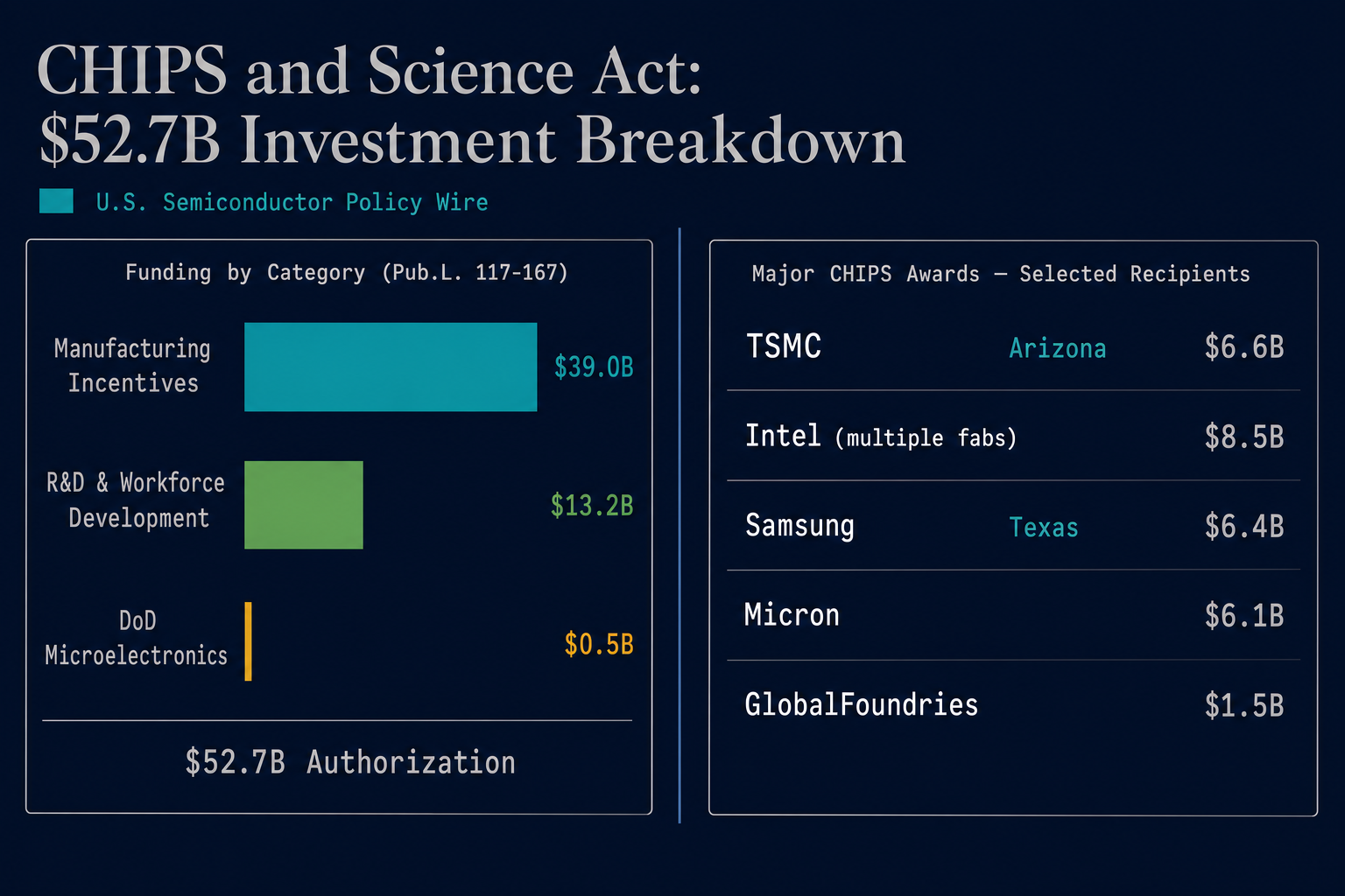
The statute allocates $39 billion to the CHIPS Program Office (CPO) for direct manufacturing incentives, grants, loans, and loan guarantees for domestic fabrication facilities, advanced packaging, and materials production. A separate 25 percent investment tax credit under Section 48D of the Internal Revenue Code applies to qualifying semiconductor manufacturing equipment costs and is not drawn from the $39 billion appropriation.
The CHIPS Research and Development Office (CRDO) received $11 billion in direct appropriations for R&D, structured across four programs: $5 billion for the National Semiconductor Technology Center (NSTC), $3 billion for the NIST Manufacturing USA Institute, $2 billion for NIST’s CHIPS R&D activities, and $1 billion for the National Advanced Packaging Manufacturing Program (NAPMP). The act separately authorizes, but does not appropriate, an additional $200 billion for the NSF, DOE, NIST, and NASA over fiscal years 2023 through 2027, of which roughly $81 billion targets NSF alone. Authorizations require separate Congressional appropriations and have not been fully funded.
The NSTC, operated as a public-private consortium, opened its Natcast operating entity in 2023. Its mandate covers prototyping, advanced test and packaging capabilities, metrology research, and supply chain verification: functions the private sector has historically under-invested in due to their pre-competitive nature.
As of early 2025, the CRDO has awarded approximately $8.3 billion against its $11 billion allocation. NSTC funding continues to be disbursed through Natcast’s growing consortium membership.
Major CHIPS Awards: What Has Been Allocated So Far
The CPO has finalized 20 awards totaling up to $33.7 billion in direct funding and up to $5.5 billion in loans as of early 2025. The four largest awards, to TSMC, Intel, Samsung, and Micron, account for the bulk of the manufacturing incentive pool.
TSMC Arizona Corporation received a finalized award of up to $6.6 billion in direct funding, announced in November 2024. The award supports a three-fab complex in Phoenix, with Fab 21 Phase 1 producing at 4nm and entering volume production in early 2025. Phase 2 will target 3nm and 2nm nodes; equipment installation is scheduled for the third quarter of 2026, with production pulled forward to 2027, roughly a year ahead of the original 2028 target. A third fab on the same Phoenix campus, targeting 2nm and the A16 process node, is expected to break ground before end of 2025, with production by end of decade. Total announced investment: $165 billion.
Intel finalized an award of $7.86 billion in November 2024, subsequently modified in August 2025 to accelerate $5.7 billion of that total ahead of schedule. The agreement covers Intel facilities in Chandler, Arizona; Rio Rancho, New Mexico; New Albany, Ohio; and Hillsboro, Oregon: spanning logic fabrication and advanced packaging. The modification removed certain workforce development milestones in exchange for the accelerated disbursement structure.
Samsung Electronics Texas received a finalized award of $4.745 billion, reduced from an initial proposed figure of $6.4 billion following Commerce’s due diligence review. The award covers Samsung’s Taylor, Texas site, where two leading-edge logic foundry fabs will target 2nm process technology and an on-site R&D fab will develop process nodes several generations ahead of production. An adjacent expansion at Samsung’s existing Austin facility covers FD-SOI production for aerospace, defense, and automotive applications.
Micron Technology received $6.165 billion in finalized awards in December 2024. New York facilities are sited at the White Pine Commerce Park in the Town of Clay, Onondaga County; Idaho facilities are in Boise. Both sites focus on leading-edge DRAM production, including High-Bandwidth Memory (HBM) capacity critical to AI accelerator supply chains. Micron subsequently reallocated approximately $1.2 billion from the New York award to accelerate its Idaho expansion. The two-decade buildout is projected to raise the U.S. share of advanced memory manufacturing from below 2 percent to approximately 10 percent by 2035.
Smaller but strategically significant awards include $1.61 billion to Texas Instruments for three analog semiconductor fabs and $1.5 billion to GlobalFoundries for expansion in Malta, New York and South Burlington, Vermont.
CHIPS Act Major Awards, Summary Table
| Recipient | Location | Award (Direct) | Node Target | Status |
|---|---|---|---|---|
| TSMC Arizona | Phoenix, AZ | $6.6B | 4nm / 3nm / 2nm / A16 | Finalized Nov. 2024 |
| Intel | Chandler AZ; Rio Rancho NM; New Albany OH; Hillsboro OR | $7.86B (modified) | Intel 18A / Intel 3 / Advanced Packaging | Finalized Nov. 2024; Modified Aug. 2025 |
| Samsung Electronics Texas | Taylor, TX; Austin, TX | $4.745B | 2nm / FD-SOI | Finalized Dec. 2024 |
| Micron Technology | Clay, NY; Boise, ID | $6.165B | Leading-edge DRAM / HBM | Finalized Dec. 2024 |
| Texas Instruments | Multiple TX/UT sites | $1.61B | Analog / Mixed-signal (65nm–180nm) | Finalized |
| GlobalFoundries | Malta, NY; South Burlington, VT | $1.5B | FD-SOI / 12nm FinFET | Finalized |
Export Controls: BIS Rules and the October 2022 Restrictions
The Bureau of Industry and Security (BIS) issued an interim final rule on October 7, 2022, amending the Export Administration Regulations to restrict exports of advanced computing integrated circuits, semiconductor manufacturing equipment, and related items to China. The rule introduced new Export Control Classification Numbers (ECCNs), including 3A090 for advanced semiconductors and 4A090 for high-performance computing systems exceeding defined performance thresholds.
BIS issued two expanded interim final rules on October 17, 2023. The first, “Implementation of Additional Export Controls: Certain Advanced Computing Items; Supercomputer and Semiconductor End Use; Updates and Corrections” (88 Fed. Reg. 73482), broadened license requirements for ECCNs 3A090 and 4A090 beyond China to approximately 40 countries in Country Groups D:1, D:4, and D:5 of the EAR. The second: “Export Controls on Semiconductor Manufacturing Items” (88 Fed. Reg. 73444), tightened restrictions on semiconductor manufacturing equipment, including deposition, etch, and lithography tools, with direct implications for ASML’s extreme ultraviolet (EUV) equipment supply to Chinese fabs.
The 2022 and 2023 rules together imposed a de facto embargo on Chinese access to sub-14nm logic fabrication technology and advanced memory manufacturing equipment. SMIC, China’s largest foundry, and CXMT, its primary DRAM producer, have been operating under the constraints of these restrictions since late 2022, limiting their process node advancement without access to ASML EUV tools or advanced etch and deposition equipment from Applied Materials, Lam Research, and KLA.
BIS issued a further update in December 2024, strengthening foundry due diligence requirements and adding Entity List designations for Chinese semiconductor tool makers attempting to replicate restricted equipment domestically. Compliance enforcement, previously criticized by the GAO as inconsistent, has expanded through BIS’s End-User Review Committee and bilateral export enforcement dialogues with the Netherlands and Japan.
The Guardrails: Restrictions on CHIPS Act Recipients
Section 9902 of the CHIPS and Science Act imposes a suite of national security conditions on all incentive recipients. The core restriction prohibits “significant transactions” involving the “material expansion” of semiconductor manufacturing capacity in a “foreign country of concern”, defined as China, Russia, Iran, and North Korea, for a period of 10 years from the date the funding agreement is finalized. A “significant transaction” is defined as one valued at $100,000 or more, or an aggregate series reaching that threshold. “Material expansion” means increasing a facility’s capacity by more than five percent.
A carve-out permits continued operation of existing legacy facilities and new legacy capacity predominantly serving the country of concern’s domestic market, where “predominantly serving” means at least 85 percent of output is consumed in that market. Legacy node definitions under the final rule: published by Commerce in September 2023, cover generally-available technologies at 28nm or above for logic, with separate thresholds for DRAM and NAND.
Recipients may not engage in joint research or technology licensing with a “foreign entity of concern” on technologies or products raising national security concerns. Recipients are barred from using CHIPS Act funds for stock buybacks, dividends, or other capital distributions. Violations trigger a full clawback of disbursed funds plus accrued interest.
The guardrail framework has created compliance complexity for TSMC and Samsung, both of which operate substantial legacy and mature-node capacity in China. TSMC’s Nanjing fab, producing at 16nm and 28nm, and Samsung’s Xi’an NAND facility required Commerce Department review under the framework before award finalization.
TSMC, Intel, Samsung: US Fab Investment Timeline
TSMC’s Arizona commitment predates the CHIPS Act. The company announced Fab 21 Phase 1 in May 2020, initially projecting $12 billion in investment and 5nm production. The CHIPS Act award accelerated the company’s expansion to three fabs and $165 billion in total committed investment, the largest announced foreign direct investment in U.S. history. Phase 1 entered volume production at 4nm in early 2025, supplying Apple, NVIDIA, and AMD. Phase 2 equipment installation begins in Q3 2026 for 3nm/2nm production in 2027. Phase 3 targets 2nm and A16 processes by end of decade.
Intel’s US Fab investment covers four states under the CHIPS agreement. The Chandler, Arizona campus (Fab 52 and Fab 62) is advancing Intel’s 18A process node, which the company positions as its return to process leadership. New Albany, Ohio is the primary site for Intel’s “Silicon Heartland” campus, targeting high-volume manufacturing at future nodes. Rio Rancho, New Mexico handles back-end packaging and test. Hillsboro, Oregon remains Intel’s primary R&D and process development center. The modified August 2025 agreement reflects Intel’s financial restructuring under CEO Lip-Bu Tan, who took over in March 2025 following Pat Gelsinger’s departure.
Samsung’s Taylor, Texas groundbreaking occurred in November 2022. Construction has faced delays; as of late 2024, reports indicated the company paused completion timelines at Taylor due to insufficient customer commitments for its U.S. foundry capacity. The CHIPS award of $4.745 billion was finalized in December 2024 despite the construction pace uncertainty. Samsung’s Austin facility, operational since 1996, continues to produce for existing customers through the buildout period.
Micron’s New York and Idaho expansions operate on a 20-year buildout horizon. The company’s Clay, New York site broke ground in April 2023. Idaho’s Boise facilities serve as the nearer-term production ramp, with the first new Boise fab accelerated under the $1.2 billion reallocation from the New York award pool.
What’s Next: Remaining Awards and Policy Milestones
The CPO has awarded approximately $33.7 billion of the $39 billion manufacturing incentive pool as of early 2025, leaving roughly $5.3 billion in uncommitted direct incentives. The Notice of Funding Opportunity for Facilities for Semiconductor Materials and Manufacturing Equipment was reopened in October 2025, with concept plans accepted through November 1, 2026, indicating Commerce continues to solicit proposals from materials suppliers and equipment manufacturers to fill gaps in the domestic supply chain upstream of wafer fabrication.
The CRDO has disbursed approximately $8.3 billion of its $11 billion R&D allocation. NSTC program awards, Design and Advanced Node (DAN) R&D awards, and NAPMP packaging awards continue on rolling schedules through NIST’s program office.
BIS export control policy remains under active revision. A December 2024 rule introduced enhanced controls targeting AI chip diffusion through third countries, addressing the loophole identified in the October 2023 framework where restricted chips were transshipped via non-restricted jurisdictions. Further tightening on gate-all-around (GAA) transistor fabrication equipment and high-bandwidth memory is anticipated as Chinese domestic development programs advance.
The Trump administration, which took office in January 2025, has maintained the CHIPS incentive disbursements while signaling review of export control architecture. Commerce Secretary Howard Lutnick indicated in February 2025 that the administration views CHIPS manufacturing awards as consistent with its domestic industrial policy priorities. The Intel agreement modification of August 2025: in which the U.S. government acquired a 10 percent equity stake as part of the accelerated disbursement structure, represents a structural departure from the grant-only model that characterized the Biden-era CHIPS awards.
Congressional authorization for remaining CRDO science appropriations has not been completed. The $174 billion in science authorizations embedded in the act’s Title II provisions have been partially appropriated in annual spending bills but remain well below the authorized ceilings.